
Rs.1,943.53cr facility will cater to high-growth sectors, says Minister
Odisha is fast emerging as a semiconductor hub, with two approved projects under the India Semiconductor Mission, including the advanced 3D Glass unit groundbreaking-inauguration of which was held on 19 April, says State Minister for Electronics & IT Dr Mukesh Mahaling.
He also elaborated on the State Government’s IT, AI, GCC and Semiconductor Policies 2025, saying these policies will drive innovation and attract investments.
Emphasising skill development, he said stipend support for engineering students is being provided to build an industry-ready workforce.
He informed that initiatives like the Blackswan Summit 2026 and growing AI investments will create jobs and strengthen Odisha’s leadership in future technologies.
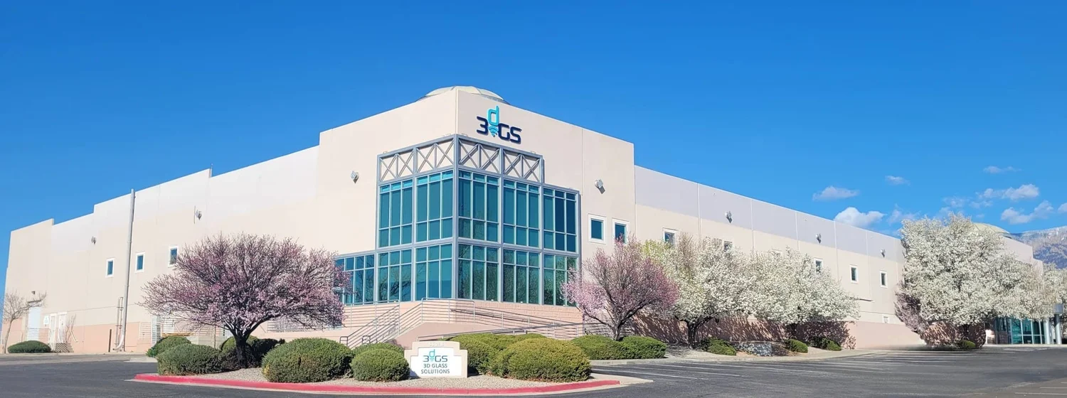
The 3D Glass project is being implemented by 3D Glass Solutions Inc (3DGS), USA, through its wholly owned Indian subsidiary Heterogeneous Integration Packaging Solutions Pvt Ltd (HIPSPL) at Info Valley in Khordha district, Bhubaneswar. It is a greenfield, vertically integrated advanced packaging and embedded glass substrate ATMP facility.
The total investment in the project is Rs.1,943.53 crore, including approved Central fiscal support of Rs.799 crore and additional State support of approximately Rs.399.5 crore, Mahaling said. The groundbreaking ceremony was held on 19 April.
The facility will cater to high-growth sectors such as data centres, Artificial Intelligence, machine learning, 5G/6G communications, automotive radar, defence electronics, aerospace applications, and photonics. Commercial production is expected to begin by August 2028, while full-scale volume production is targeted by August 2030.
The facility is expected to produce 70,000 glass panels annually, along with 50 million assembled units and around 13,000 advanced 3DHI modules. Fiinews.com


